Designing printed circuit boards (PCBs) was once expensive and complex, requiring specialized software and expertise. Today, professional-grade PCB design tools are available for free—accessible to hobbyists, students, and professionals. This comprehensive guide explores the best free PCB design software available, comparing features, capabilities, and use cases.
What is PCB Design Software?
PCB design software allows engineers to:
- Create schematics - Design electronic circuits with symbols and connections
- Design layouts - Arrange components on physical boards
- Route traces - Draw connections between components
- Generate files - Produce manufacturing files (Gerber, Drill, etc.)
- Manage libraries - Access and create component symbols and footprints
- Check rules - Verify designs for electrical and manufacturing errors
Why Use Free PCB Design Software?
Cost Savings
Professional PCB software can cost $1000-5000+. Free tools eliminate this barrier.
Accessibility
Anyone can design and manufacture PCBs—no expensive licenses required.
Open Source
Many free tools are open source with active communities contributing improvements.
No Limitations
Modern free software matches or exceeds paid alternatives in features and capabilities.
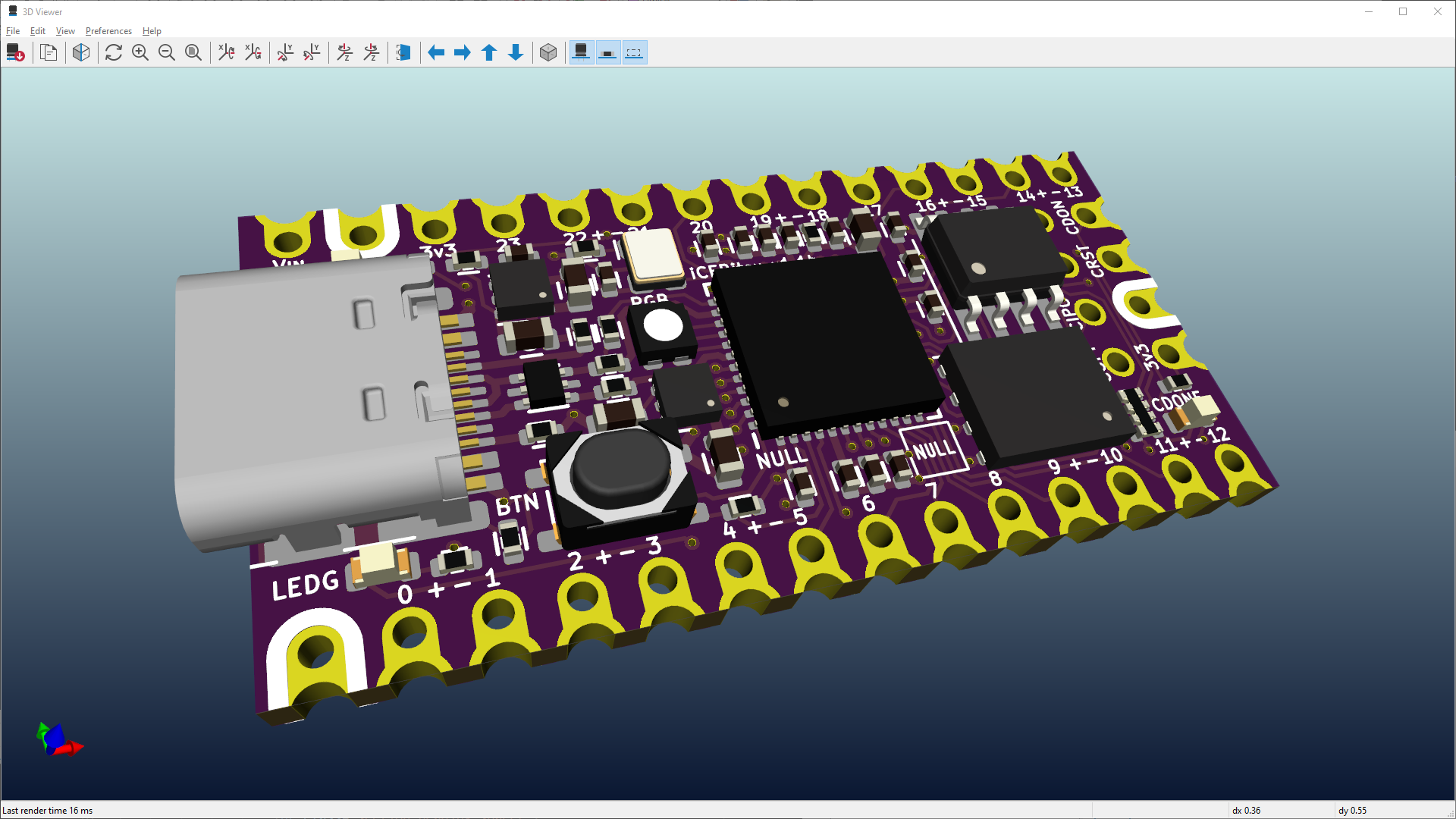
KiCad: Professional-Grade Free PCB Design
Best For: Complex projects, professional production, advanced users
Overview
KiCad is the gold standard in free PCB design software. It's powerful, open-source, and used by professionals worldwide for everything from hobby projects to commercial products.
Key Features:
- Schematic Editor - Draw unlimited hierarchical schematics
- PCB Layout - 32-layer board support (expandable)
- 3D Viewer - Realistic 3D visualization of your PCB
- Footprint Editor - Create custom component packages
- Symbol Library - Massive built-in component library
- Design Rule Check - Verify design integrity automatically
- Gerber Export - Production-ready manufacturing files
- Multi-platform - Windows, Mac, Linux
Installation:
- Visit kicad.org
- Download latest version (currently 8.0+)
- Install and launch
- Start with built-in tutorials
Workflow:
1. Create New Project
   └─ Creates folder with all project files

2. Design Schematic
   └─ Add symbols, draw connections, add values

3. Design PCB Layout
   └─ Place footprints, route traces, add vias

4. Check Design
   └─ Run DRC (Design Rule Check)

5. Generate Gerber Files
   └─ Export production files for manufacturer

6. Order PCBs
   └─ Send to PCB fab (JLCPCB, PCBWay, etc.)
Simple ESP32 Project Example:
Schematic Elements:
- ESP32 Module
- 3.3V Voltage Regulator
- USB Connector
- Reset Button
- Boot Button
- Power LED
- Decoupling Capacitors

PCB Layout:
- 4-layer board (Power, Ground, Signal layers)
- Trace width: 8 mil (0.2mm)
- Via size: 10 mil (0.25mm)
- Minimum clearance: 5 mil (0.125mm)
Pros:
- Professional-grade capabilities
- Unlimited board size and complexity
- Excellent 3D visualization
- Strong community support
- Completely free, open source
Cons:
- Steeper learning curve for beginners
- Interface can feel overwhelming initially
- Requires local installation
Learning Resources:
- Official KiCad tutorials
- YouTube channels: Paul McCartney, Contextual Electronics
- Community forums: KiCad forums, Reddit r/KiCad
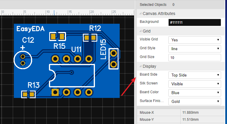
EasyEDA: Online PCB Design Made Simple
Best For: Beginners, quick prototypes, cloud-based workflow, direct PCB ordering
Overview
EasyEDA is a cloud-based PCB design platform requiring no installation. Perfect for beginners and those wanting to jump straight into ordering PCBs.
Key Features:
- Cloud-Based - Access from any browser, auto-saves
- Schematic Editor - Intuitive drag-and-drop interface
- PCB Layout - Multi-layer support (up to 16 layers)
- 3D Viewer - Real-time 3D visualization
- Large Component Library - Real components with 3D models
- SPICE Simulation - Test circuits before building
- Design Rule Check - Automatic error detection
- Integrated Ordering - Order directly from EasyEDA partner (JLCPCB)
- Free and Pro Plans - Free version is excellent
Getting Started:
- Visit easyeda.com
- Create free account
- Start new project
- Choose schematic or PCB design
Workflow:
1. Create Account (Free)
   └─ Email verification

2. New Project
   └─ Select Schematic or PCB

3. Design in Browser
   └─ Real-time collaboration
   └─ Auto-save to cloud

4. Simulate (Optional)
   └─ Test circuit behavior
   └─ Verify functionality

5. Export or Order
   └─ Export Gerber files
   └─ Or order PCBs directly
Unique Features:
SPICE Simulation
Test your circuit before manufacturing:
// Example: LED Current Limiting
- 5V power supply
- LED (Vf = 2V, If = 20mA max)
- Calculate resistor: R = (5V - 2V) / 20mA = 150Ω
- Simulate to verify
Direct Integration with JLCPCB
Seamlessly order PCBs:
- Designs sync directly to JLCPCB
- Get instant quotes
- Order in minutes
Pros:
- No installation required
- Beginner-friendly interface
- Cloud-based with auto-save
- Built-in SPICE simulation
- Direct PCB ordering integration
- Collaborative features
- Excellent for quick projects
Cons:
- Limited by browser/internet connection
- Pro features require subscription
- Less control than desktop tools
- Component library can be overwhelming
Free vs Pro:
| Feature | Free | Pro |
|---|---|---|
| Projects | Unlimited | Unlimited |
| Schematic | ✓ | ✓ |
| PCB Layout | ✓ | ✓ |
| Simulation | Limited | ✓ |
| Libraries | Large | Larger |
| Export | ✓ | ✓ |
Fritzing: Visual PCB Design for Beginners

Best For: Beginners, educational projects, breadboard prototyping, documentation
Overview
Fritzing is perfect for beginners because it uses familiar breadboard and component visuals. Great for documenting Arduino and Raspberry Pi projects.
Key Features:
- Breadboard View - Visual breadboard layout
- Schematic View - Traditional schematic drawing
- PCB View - Convert to PCB layout
- Large Component Library - Arduino, sensors, common parts
- Export Options - PNG, PDF, SVG, Gerber
- Educational Focus - Perfect for teaching electronics
Installation:
- Visit fritzing.org
- Download for your platform (Windows, Mac, Linux)
- Install and launch
Unique Workflow:
1. Breadboard View
   └─ Drag components
   └─ Draw wires (visual)
   └─ See actual circuit layout

2. Schematic View
   └─ Auto-generated from breadboard
   └─ Or design from scratch

3. PCB View
   └─ Convert to PCB layout
   └─ Route traces
   └─ Export for manufacturing
Example: Arduino LED Circuit
Breadboard View:
[Arduino] ─── [LED] ─── [Resistor] ─── GND

Schematic View:
Pin13 → [Resistor 220Ω] → [LED] → GND

PCB View:
(Two-layer board with Arduino pinout)
Pros:
- Extremely beginner-friendly
- Visual breadboard makes learning easier
- Perfect for Arduino/Raspberry Pi documentation
- Great for educational purposes
- Free and open source
Cons:
- Limited for complex designs
- PCB layout capabilities less advanced
- Component library can be incomplete
- Slower development than alternatives
Other Free PCB Design Tools
Autodesk Eagle (Free Personal Use)
Best For: Professional-quality designs with fewer board size restrictions than some alternatives
- Two free projects (up to 80cm²)
- Industry standard in many companies
- Large community and component library
- Cross-platform (Windows, Mac, Linux)
Altium Designer Viewer (Free)
Best For: Viewing and editing professional designs
- View existing designs
- Make limited edits
- Learn from professional schematics
PCBWeb (Free Online)
Best For: Quick, simple designs without installation
- Browser-based design
- Free tier with limitations
- Integration with PCB ordering
LibrePCB (Emerging)
Best For: Modern, open-source alternative to KiCad
- New, actively developed
- Cross-platform
- Open source
- Still gaining community adoption
Comparison Table
| Software | Best For | Installation | Learning Curve | PCB Complexity | Cost |
|---|---|---|---|---|---|
| KiCad | Professional projects | Local install | Moderate-High | Unlimited | Free |
| EasyEDA | Quick prototypes | Online only | Low | Medium-High | Free/Pro |
| Fritzing | Beginners/Learning | Local install | Very Low | Low-Medium | Free |
| Eagle | Professional use | Local install | Moderate | Limited free | Free (limited) |
PCB Design Workflow: From Idea to Production
Step 1: Plan Your Design
- Sketch circuit on paper
- List all components
- Determine board size and requirements
Step 2: Create Schematic
- Add components from library
- Draw connections
- Add reference designators (R1, C1, etc.)
- Add component values
Step 3: Perform Electrical Checks
- Check for unconnected pins (floating nodes)
- Verify power distribution
- Check signal routing
Step 4: Design PCB Layout
- Place components strategically
- Minimize trace lengths
- Separate analog and digital grounds (if applicable)
- Route critical signals carefully
Step 5: Route Traces
- Connect components with traces
- Use vias for multi-layer connections
- Maintain trace width rules
- Avoid sharp angles
Step 6: Design Rule Check (DRC)
- Run automated design checks
- Fix clearance violations
- Verify manufacturing requirements
Step 7: Generate Gerber Files
- Export manufacturing files
- Include drill file
- Add silkscreen
- Generate file preview
Step 8: Order PCBs
- Choose manufacturer (JLCPCB, PCBWay, Oshpark)
- Upload Gerber files
- Get instant quote
- Order and wait (usually 5-14 days)
Best Practices for PCB Design
Component Placement
- Group related components
- Place high-speed components close together
- Keep power supplies near supply points
- Minimize current loop areas
Trace Routing
- Use appropriate trace widths (thicker for power)
- Avoid acute angles (use 45° or 90°)
- Separate analog and digital traces
- Keep critical signals short
Power Distribution
- Multiple ground planes for low impedance
- Adequate power traces
- Decoupling capacitors near power pins
- Proper fusing and protection
Thermal Management
- Heat sinks for high-power components
- Thermal vias under components
- Copper pour for heat distribution
- Adequate spacing for ventilation
Creating Custom Footprints and Symbols
When to Create Custom Footprints:
- Using specialized or rare components
- Custom connectors
- Non-standard packaging
How to Create (KiCad):
1. Open Footprint Editor
2. Create new footprint
3. Add pads with correct dimensions
4. Add silkscreen outline
5. Set electrical properties
6. Save to library
Resources and Learning
Tutorials:
- YouTube: Contextual Electronics, Paul McCartney
- Official documentation for each tool
- Udemy and Coursera courses
Communities:
- Reddit: r/pcb, r/electronics
- Official forums for each tool
- GitHub repositories with examples
Component Resources:
- Datasheets (pdf.datasheetspdf.com)
- Octopart.com for component information
- Electronics reference sites
PCB Ordering and Manufacturing
Top PCB Manufacturers (Free Shipping Options):
- JLCPCB - $2 for 5 boards, 48-hour turnaround
- PCBWay - Various options, competitive pricing
- Oshpark - Premium quality, higher cost
- SeeedStudio Fusion - Good quality, reasonable pricing
Typical Costs:
- PCB prototype: $2-10 (5 boards)
- Component assembly: $0.50-2 per board
- Shipping: $5-15 globally
Real-World Example: Arduino Shield Design
Let's design a simple ESP32 WiFi shield:
Schematic:
Components:
- ESP32 Module
- 3.3V voltage regulator (AMS1117)
- USB Type-C connector
- Reset button
- Boot button
- Status LED (red)
- Power LED (green)
- Decoupling capacitors (100nF, 10µF)
- 2.4GHz antenna connector
Layout Considerations:
- Antenna placed at board edge
- Power supply on left side
- GPIO header on right side
- USB connector on bottom
- 4-layer board for optimal performance
File Generation:
- Gerber files (.gbr)
- NC Drill file (.txt)
- Assembly drawing
- Bill of Materials (BOM)
Conclusion
The era of expensive PCB design software is over. Today's free tools rival professional software costing thousands of dollars. Whether you're a beginner using Fritzing, a maker using EasyEDA, or an advanced designer using KiCad, you have access to world-class PCB design capabilities.
Start with the tool that matches your needs:
- Just learning? Use Fritzing
- Want quick prototypes? Use EasyEDA
- Building professional projects? Use KiCad
The barrier to entry for PCB design has never been lower. Combined with cheap PCB manufacturing (as low as $2-5), you can now design, manufacture, and iterate on custom hardware in days instead of months.
Ready to design your first PCB? Check out our Arduino and ESP32 projects for circuit inspiration, then build your custom board! 🔧